# Large-area metalens
Metalenses are a new class of optical devices that have recently gained a lot of attention in the field of optics and photonics. They are essentially flat lenses made of thin layers of nanostructures that can focus light in a manner that is similar to traditional lenses, but with a number of unique advantages. Metalenses are capable of achieving high resolution imaging, can be easily integrated with other optical components, and have the potential to significantly reduce the size and weight of traditional lens systems. Additionally, metalenses can be designed to operate across a wide range of wavelengths, making them useful in a variety of applications, such as in imaging, sensing, and communications. The development of metalenses has opened up exciting new opportunities in the field of optics and is likely to have a significant impact on a wide range of industries in the near future.
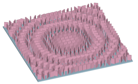
In this example, we use Tidy3D to simulate a very large dielectric metalens. We base this example off of the recent paper from Khorasaninejad et al. titled Metalenses at visible wavelengths: Diffraction-limited focusing and subwavelength resolution imaging (opens new window), which was recently published in Science. In this paper, a 2-dimensional array of dielectric structures is used as a lens to focus transmitted light to a single position directly above the device.
Typically, these structures are simulated by simulating each dielectric unit cell individually to compute a phase and amplitude transmittance for each cell. While this approach makes for an approximation of the overall device performance, it would be useful to be able to simulate the entire device as a whole to capture the entire physics. However, a simulation of this scale requires several hours or days to do with a conventional CPU-based FDTD. With Tidy3D, we are able to complete the entire simulation in about 1 minute!
First, we’ll show a simple approach for computing fields on the focal plane by simply placing a FieldMonitor (opens new window) at the focal plane to record the fields. However, the focal plane is several wavelengths away from the structure, which means that the above setup will involve simulating fields propagating through lots of empty space. Therefore, we will also show how one can instead record the near fields on a large surface just above the structure, and then project them to the focal plane without actually simulating the fields in the empty region in between, leading to a further improvement in the already-impressive simulation speed.
To view the full example in Python, please click here (opens new window).
To view the example in our web GUI, please click here (opens new window).