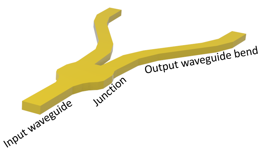
# Waveguide Y junction
Power splitters such as Y-junctions are widely used in photonic integrated circuits across different applications. When designing a power splitter, we aim to achieve a flat broadband response, low insertion loss, and compact footprint. At the same time, the design needs to comply with the fabrication resolution and tolerance.
In this example, we demonstrate the modeling of a Y-junction for integrated photonics. The designed device shows an average insertion loss below 0.2 dB in the wavelength range of 1500 nm to 1600 nm. At the same time, it has a small footprint. The junction area is smaller than 2
To view the full example in Python, please click here (opens new window).